 Products Center
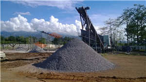
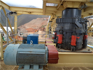
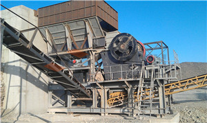
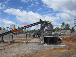
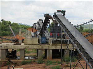
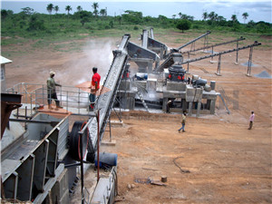
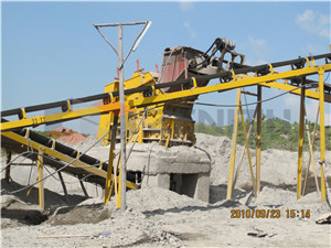
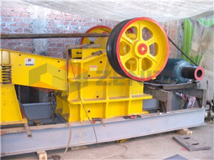
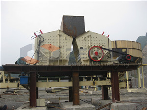
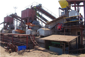
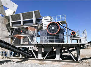
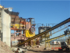
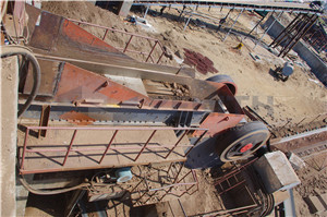
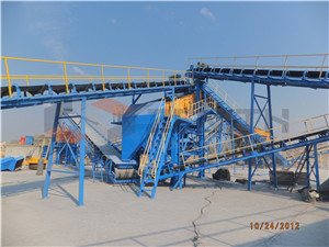
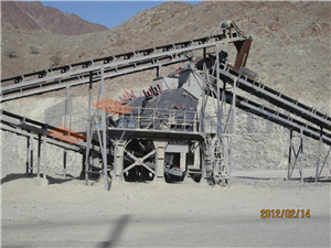
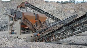
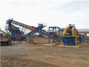
 Stone Crusher
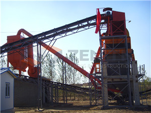
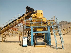
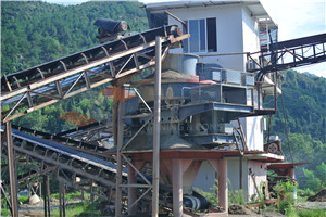
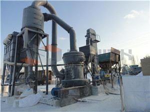
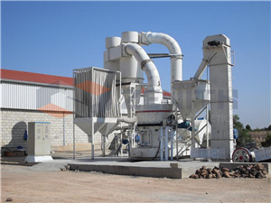
Grinding Mill
Optional Equipment
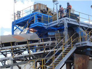
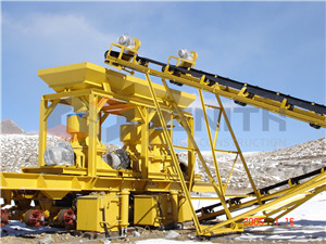
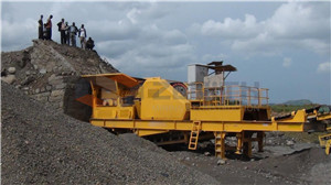
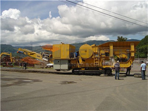
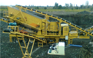
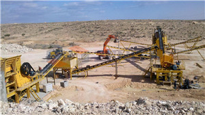
Mobile Crusher
Knowledge Hall
Crushers FAQ
Grinding Mills FAQ
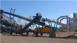
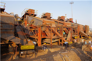
Mining Equipments
Solution
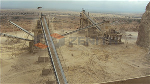
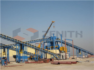
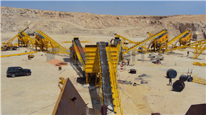
Stone Crushing
Sand Making
Ore Processing
Grinding Plant
Construction Building Material
grinding process in mems
WAFER EDGE GRINDING PROCESS (Wafer Edge Profiling ...
Innovative Process Solutions. This application note discusses the Edge Grinding of hard, brittle materials that are common to semiconductor, MEMS, LEDs, and other ...

Axus: Semiconductor & MEMS/Nanofabrication …
Axus Technology provides leading edge equipment and process solutions for surface processing applications, including polishing, grinding and lapping
MEMS Grows Up - MICROmanufacturing | Where …
Analysts: 2010 the year MEMS comes of age. As the global market for microelectromechanical systems rebounded from the first official recession in its 30 …
MEMS Fab Processing Capabilities | 4" & 6 inch …
Micralyne has MEMS capabilities for microfabrication, packaging, assembly and characterization of MEMS devices on 4-inch and 6-inch wafers.
Search | MICROmanufacturing
Midwest Industrial Tool Grinding Inc., Hutchinson, Minn., is a first-time finalist in two categories for the Minnesota Business 2014 Manufacturing Awards.
MEMS Foundry Contract Manufacturing – …
Innovative Micro Technology (IMT) -- MEMS foundry/contract manufacturer, serving fabless and fab-light MEMS companies for MEMS wafer fabrication/foundry service with ...
Advanced Materials Processing Products - …
Learn more about Lapmaster's advanced materials processing (AMP) products: lapping machines, polishing machines, wafer edge grinding, wafer planarization machines and ...
MEMS & SENSORS PACKAGING - SEMI - Home | SEMI.ORG
Outline 1. Brief presentation of ASE Group 2. Overview of MEMS packaging 3. ASE MEMS packaging background and examples 4. Evolution to wafer level packaging (WLP)
Titanium and Titanium Alloys - Cutting, Grinding …
This article provides a guide to the machining of titanium alloys. Some details are provided for operations including cutting, grinding, surface grinding, turning ...
Lid & Optical Seal Solutions | AI Technology, Inc.
AIT engineered and designed several innovative lid-sealing solutions for optical, thermal, EMI and commercial component and module packaging with outanding cost ...
Micro-Machining - Georgia Institute of Technology
Photolithography Process DescriptionPhotolithography Process Description • The wafers are chemically cleaned to remove particulate matter, organic ionic and ...
Wafer dicing - Wikipedia, the free encyclopedia
Wafer dicing is the process by which die are separated from a wafer of semiconductor following the processing of the wafer. The dicing process can be accomplished by ...
Flow meter,Fluidizing conveyor,Ball mill,Grinding …
Vibrating bin discharger with dual outlets,Pipeline mixer,Colloid mixer, Homomixer,AGI mixer,Stainless steel heavy-duty mixer,Compact spray dryer,Dryer-cooler ...
Loadpoint - Precision Dicing Saws, Dicing Blades …
Loadpoint develop and manufacture high precision dicing saws and machining systems for Semiconductors, MEMs, PZT and Piezo materials, Photonics and related industries.
Electrochemical machining [SubsTech] - main …
Electrochemical machining is a process of a selective dissolution of the anodically connected work piece material submerged in an electrolyte together with an ...
Machining Of Boron Carbide (B4C) - Process, …
Boron Carbide is a useful engineering ceramic that possesses high hardness and high temperature stability. It has many industrial applications, but machining it to ...
About Composites/Plastics - Learn About …
Learn About Plastic and Composite Materials, About Composites/Plastics
Nanotechnology Companies - By Location
Nanotechnology Businesses sorted by location. In some instances, the business has many locations - in these cases, we have included the corporate headquarters, and ...
4Semi - Used and Surplus Semiconductor …
Marketplace for used semiconductor manufacturing equipment. Searchable tree of available products, with descriptions, specifications, photos, and asked prices.
DESIGN AND PROCESS OPTIMIZATION OF THROUGH SILICON …
DESIGN AND PROCESS OPTIMIZATION OF THROUGH SILICON VIA INTERPOSER FOR 3D-IC INTEGRATION Pejman Monajemi, Michael Newman, Cyprian Uzoh, …
Nanotech Now - Nanotechnology
A directory listing of business nanotechnology programs ... Home > Directory > Nanotechnology Business Sites - Sorted by Name. Nanotechnology Business Programs
Selecting Diamond Blades - SMART CUT - UKAM
selecting diamond blades, diamond blades for photonics, precision optics, diamond slicing blades, precision diamond blades with smart cut technology for ultra hard ...
Datasheet Directory - GlobalSpec
Browse GlobalSpec's Datasheet directory to locate information and specifications for more than 8 million products. The archive is organized by product area; view ...
Product Announcements - GlobalSpec
Searchable Engineering Catalogs on the Net. Hundreds of thousands of products from hundreds of suppliers of sensors, actuators, and more, all with searchable specs.
Faculty Openings - Indian Institute of Technology …
Faculty Openings The Institute invites applications from Indian nationals, possessing excellent academic background, commitment to quality teaching and ...
Micro-Machining - Georgia Institute of Technology
Photolithography Process DescriptionPhotolithography Process Description • The wafers are chemically cleaned to remove particulate matter, organic ionic and ...
Wafer dicing - Wikipedia, the free encyclopedia
Wafer dicing is the process by which die are separated from a wafer of semiconductor following the processing of the wafer. The dicing process can be accomplished by ...
Flow meter,Fluidizing conveyor,Ball mill,Grinding …
Vibrating bin discharger with dual outlets,Pipeline mixer,Colloid mixer, Homomixer,AGI mixer,Stainless steel heavy-duty mixer,Compact spray dryer,Dryer-cooler ...
Loadpoint - Precision Dicing Saws, Dicing Blades …
Loadpoint develop and manufacture high precision dicing saws and machining systems for Semiconductors, MEMs, PZT and Piezo materials, Photonics and related industries.
Electrochemical machining [SubsTech] - main …
Electrochemical machining is a process of a selective dissolution of the anodically connected work piece material submerged in an electrolyte together with an ...
Machining Of Boron Carbide (B4C) - Process, …
Boron Carbide is a useful engineering ceramic that possesses high hardness and high temperature stability. It has many industrial applications, but machining it to ...
About Composites/Plastics - Learn About …
Learn About Plastic and Composite Materials, About Composites/Plastics
Nanotechnology Companies - By Location
Nanotechnology Businesses sorted by location. In some instances, the business has many locations - in these cases, we have included the corporate headquarters, and ...
4Semi - Used and Surplus Semiconductor …
Marketplace for used semiconductor manufacturing equipment. Searchable tree of available products, with descriptions, specifications, photos, and asked prices.
DESIGN AND PROCESS OPTIMIZATION OF THROUGH SILICON …
DESIGN AND PROCESS OPTIMIZATION OF THROUGH SILICON VIA INTERPOSER FOR 3D-IC INTEGRATION Pejman Monajemi, Michael Newman, Cyprian Uzoh, …
- Last Product: suitable layout of the plant and production method
- Next Product: aluminium manganese process
RD Equipments
- line production characteristics
- french fry uk production line manufacturers
- product information mantel is designed to protect the cone crusher
- quartzite quarry processing in silica
- material processing grinding
- stage of process of silica sand
- how to solve the problems encountered in cement production
- machine used for crashing gabagge to useful products
- celestite processing plant in pakistan
- asphalt production