 Products Center
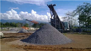
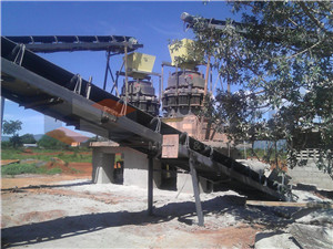
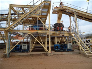
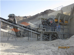
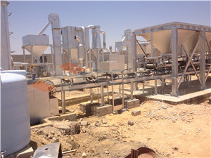
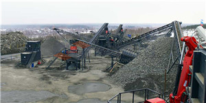
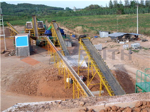
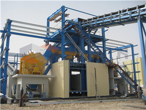
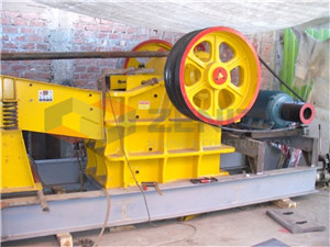
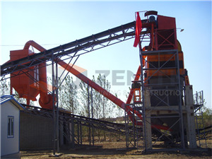
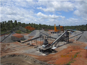
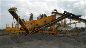
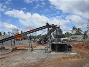
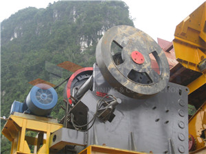
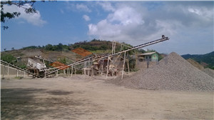
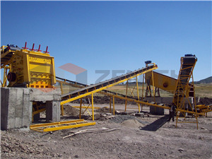
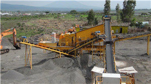
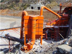
 Stone Crusher
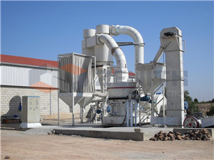
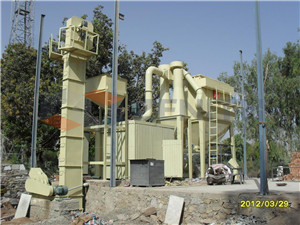
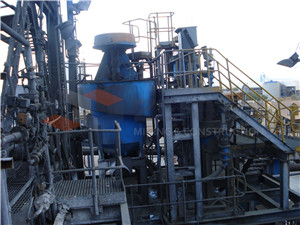
Grinding Mill
Optional Equipment
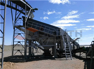
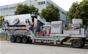
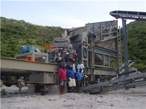
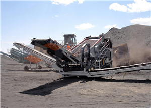
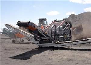
Mobile Crusher
Knowledge Hall
Crushers FAQ
Grinding Mills FAQ
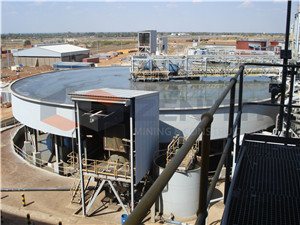
Mining Equipments
Solution
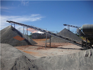
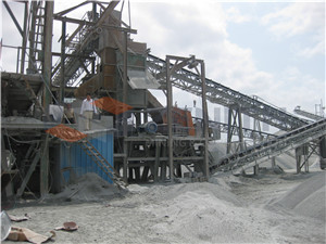
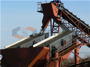
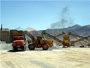
Stone Crushing
Sand Making
Ore Processing
Grinding Plant
Construction Building Material
wafer grinding process
Wafer backgrinding - Wikipedia, the free …
Wafer backgrinding is a semiconductor device fabrication step during which wafer thickness is reduced to allow for stacking and high density packaging of integrated ...
Wafer (electronics) - Wikipedia, the free …
In electronics, a wafer (also called a slice or substrate[1]) is a thin slice of semiconductor material, such as a silicon crystal, used in the fabrication of ...
Wafer Reclaim Processing - Wet Process Equipment, Wet ...
© MT Systems 2007 Page 1 Update 06/08/07 Wafer Reclaim Processing Introduction Wafer reclaim is typically defined as “a silicon wafer that has been processed, then ...
What is back grinding - Kansas State University
What is back grinding? The challenges facing back grinding… Back grinding processes; Machine configuration; Grinding wheels; 4. Effects of back grinding process on ...
Service Overview | Syagrus Systems - Wafer …
Syagrus Systems provides wafer grinding, dicing inspection and packaging services to the semiconductor industry. Contact us to learn more.
Axus Technology – CMP Foundry and Process …
Axus Technology provides leading edge equipment and process solutions for surface processing applications, including polishing, grinding and lapping
Glossary of Semiconductor Terms - Brigham …
Active Si layer - silicon layer on top of the buried oxide in SOI substrates. learn more. Adhesion - ability of materials to stick (adhere) to each other.
Silicon Materials – Silicon Wafer Manufacturing …
Silicon Wafer Manufacturing For Semiconductor, Nano Technology, MEMS, LED, and Other Technologies
Mixing Pulverizers Manufacturers, spices grinding …
Gurkirpa Industries - Mixing Pulverizers Manufacturers, spices grinding machines, chemical mixers and crushers, Food Processing Machinery Manufacturer in India ...
Metallographic Specimen Preparation Basics
Metallographic Specimen Preparation Basics www.metallographic By . Donald C. Zipperian, Ph.D. Pace Technologies . Metallography is the study of a materials ...
Applications Example | Dicing - DISCO Corporation
A simplified process with less tape mounting compared to the ring grinding process-Frame handling reduces the risk of breakage when handling thin wafers
Wafer Services | SVM - Silicon Valley …
SVM specializes in offering a wide variety of industry standard, complex and unique wafer processing solutions for semiconductor, MEMS, and other applications.
Axus Technology – CMP Foundry and Process …
Axus Technology provides leading edge equipment and process solutions for surface processing applications, including polishing, grinding and lapping
Glossary of Semiconductor Terms - Brigham …
Active Si layer - silicon layer on top of the buried oxide in SOI substrates. learn more. Adhesion - ability of materials to stick (adhere) to each other.
Wafer & Die Visual Inspection | Syagrus Systems
Syagrus Systems provides wafer grinding, dicing inspection and packaging services to the semiconductor industry
Thin Wafer Technology - SPIL - Welcome to SPIL
Application: Wafer thinning technology has become very important as the demand for ultra-thin die used in stacked packages, IC cards and other applications are ...
Silicon Materials – Silicon Wafer Manufacturing …
Silicon Wafer Manufacturing For Semiconductor, Nano Technology, MEMS, LED, and Other Technologies
TSV Process Variations for 2.5 and 3D Semiconductor …
TSV Process Variations •Via-first integration forms TSV holes in the basic silicon wafer prior to front-end semiconductor processing. •Via-middle integration ...
Strasbaugh design and manufacturing of …
Strasbaugh is a world class manufacturer of innovative, reliable, high-yield CMP, polishing and grinding solutions. Our products serve multiple high-tech markets ...
Silicon Information - Process Specialties Inc
Process Specialties offers custom wafer processing services to the Semiconductor, MEMS and Military/Aerospace industries
Flip Chip Power MOSFET: A New Wafer Scale Packaging …
Flip Chip Power MOSFET: A New Wafer Scale Packaging Technique Aram Arzumanyan, Ritu Sodhi, Dan Kinzer, Hazel Schofield, Tim Sammon International Rectifier Corporation,
Silicon wafer producers and suppliers - Where to …
link page: silicon wafer producers, FZ, CZ, EPI, silicon wafer suppliers, hyperpure silicon
Semiconductor Industry Suppliers
Semiconductor Today : the first choice for professionals who demand timely, focused, top-quality coverage of the compound semiconductor industry.
Glass Wafers & Thin Glass Substrates: SCHOTT …
SCHOTT is the world’s leading supplier of thin and ultra-thin glass wafers and substrates made of different materials in sizes of between 4" and 12" with various ...
6.1.2 Silicon Crystal Growth - uni-kiel.de
We recognize one reason why practically only As, P, and B is used for doping! Their segregation coefficient is close to 1 which assures half-way homogeneous ...
Unisem: Unisem Batam, Unisem Chengdu, Unisem …
Unisem Wales, Unisem Europe: IC assembly, Package testing, IC packaging, Device packaging, MEMS, IC prototype, Wafer dicing, Semiconductor packageing, Tape …
Process piping guide_r2 - SlideShare
2013-11-10 · Process piping guide_r2 Document Transcript. LANL Engineering Standards Manual PD342 Chapter 17 Pressure Safety Section D20-B31.3-G, ASME B31.3 Process ...
Applications Example | Dicing - DISCO Corporation
A simplified process with less tape mounting compared to the ring grinding process-Frame handling reduces the risk of breakage when handling thin wafers
Wafer Services | SVM - Silicon Valley …
SVM specializes in offering a wide variety of industry standard, complex and unique wafer processing solutions for semiconductor, MEMS, and other applications.
Axus Technology – CMP Foundry and Process …
Axus Technology provides leading edge equipment and process solutions for surface processing applications, including polishing, grinding and lapping
Glossary of Semiconductor Terms - Brigham …
Active Si layer - silicon layer on top of the buried oxide in SOI substrates. learn more. Adhesion - ability of materials to stick (adhere) to each other.
Wafer & Die Visual Inspection | Syagrus Systems
Syagrus Systems provides wafer grinding, dicing inspection and packaging services to the semiconductor industry
Thin Wafer Technology - SPIL - Welcome to SPIL
Application: Wafer thinning technology has become very important as the demand for ultra-thin die used in stacked packages, IC cards and other applications are ...
Silicon Materials – Silicon Wafer Manufacturing …
Silicon Wafer Manufacturing For Semiconductor, Nano Technology, MEMS, LED, and Other Technologies
TSV Process Variations for 2.5 and 3D Semiconductor …
TSV Process Variations •Via-first integration forms TSV holes in the basic silicon wafer prior to front-end semiconductor processing. •Via-middle integration ...
Strasbaugh design and manufacturing of …
Strasbaugh is a world class manufacturer of innovative, reliable, high-yield CMP, polishing and grinding solutions. Our products serve multiple high-tech markets ...
Silicon Information - Process Specialties Inc
Process Specialties offers custom wafer processing services to the Semiconductor, MEMS and Military/Aerospace industries
- Last Product: process of crushing plant
- Next Product: kaolin processing factory in u s a